| Brief Bio of the Speaker | Prof. David Tománek studied Physics in Switzerland and received his Ph.D. from the Free University in Berlin. While holding a position as Assistant Professor of Physics in Berlin, he got engaged in theoretical research in Nanostructures at the AT&T Bell Laboratories and the University of California at Berkeley. He established the field of Computational Nanotechnology at Michigan State University, where he holds a position as Full Professor of Physics. His scientific expertise lies in the development and application of numerical techniques for structural, electronic and optical properties of surfaces, low-dimensional systems and nanostructures. Since he was working on his PhD Thesis, he promoted the use of computer simulations to understand atomic-level processes at surfaces and in atomic clusters. Witnessed in several hundred publications and invited talks are his results on the electronic structure, mechanical, thermal, and optical properties, as well as quantum conductance of nanostructures. His contributions to Computational Nanotechnology, in particular in the field of fullerenes and nanotubes, have been rewarded by a Fellowship of the American Physical Society, the Alexander-von-Humboldt Foundation Distinguished Senior Scientist Award and the Japan Carbon Award for Life-Time Achievement. |
Abstract | If graphene had a band gap, it would probably be the optimum 2D system for electronics applications. Layered transition metal dichalcogenides (TMDs) with a robust intrinsic band gap appear as the next-best alternative. Only after a long search, however, optimum strategies have been devised to make low-resistance, ohmic contacts to TMDs [1]. In the meantime, a new class of 2D semiconductors has been rapidly gaining attention, namely layered black phosphorus and related phosphorene monolayers [2]. These 2D systems display a tunable, direct fundamental band gap and thus are ideal candidates for optoelectronics applications. Recent Quantum Monte Carlo (QMC) calculations show that the inter-layer bonding, while weak, is not well described by dispersive van der Waals (vdW) interactions [3]. QMC results differ qualitatively from vdW-enhanced DFT functionals and the common designation of similar systems as “van der Waals solids” is strictly incorrect. Also other group V systems including monolayers of AsxP1-x [4], IV-VI compounds such as SiS [5] with the same average valence, and related 2D phosphorus carbide [6] share the same nonplanarity of their structure with phosphorene. Same as in phosphorene, the fundamental band gap in these systems depends sensitively on the number of layers and in-layer strain. Surprisingly, the story of group V semiconductors does not end with layered 2D systems. A previously unknown 1D structure of coiled phosphorus, shown in Fig. 1, represents the most stable P allotrope to date. The predicted structure [7] has recently been synthesized and contained inside carbon nanotubes [8]. In all cases, predictive ab initio calculations provide a useful guidance to experimental studies. References: [1] Jie Guan, Hsun-Jen Chuang, Zhixian Zhou, and David Tománek, ACS Nano 11, 3904 (2017). [2] H. Liu et al. ACS Nano 8, 4033(2014). [3] L. Shulenburger, A.D. Baczewski, Z. Zhu, J. Guan, and D. Tománek, Nano Lett. 15, 8170 (2015). [4] Zhen Zhu, Jie Guan, and David Tománek, Nano Lett. 15, 6042 (2015). [5] Zhen Zhu, Jie Guan, Dan Liu, and David Tománek, ACS Nano 9, 8284 (2015). [6] Jie Guan, Dan Liu, Zhen Zhu, and David Tománek, Nano Lett. 16, 3247 (2016). [7] Dan Liu, Jie Guan, Jingwei Jiang, and David Tománek, Nano Lett. 16, 7865 (2016). [8] Jinying Zhang et al.Angew. Chem. Int. Ed. 56, 1850-1854 (2017). 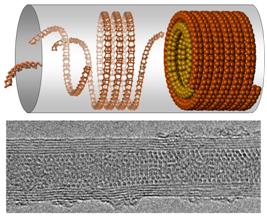
Figure 1. Top: Proposed formation mechanism of a helical phosohorus coil (Ref. [4]). Bottom: TEM micrograph of the coil embedded in a nanotube.(Ref. [5]). |